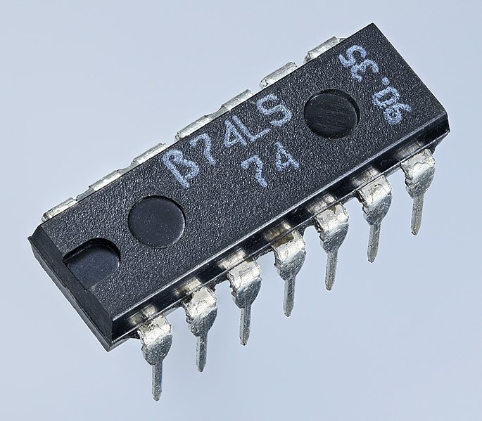
Flip-flops are widely used electronic components and are essential to most circuits. It is therefore crucial to have a thorough understanding of their behavior. To simplify the course, I will use the IEC symbols for flip-flops (European standards) rather than Anglo-Saxon symbols, for example.
When an input is inverted (usually denoted with a – above the variable), I will symbolize it by ![]()
A flip-flop is asynchronous when it does not depend on the clock signal (Clock or CLK). Therefore, a synchronous reset will only take effect on the active edge of the next clock pulse.
The RS Flip-Flop
The RS flip-flop is a very common logic circuit used in digital electronics to store a binary information bit. It consists of two NOR gates or two NAND gates, which are connected to create a positive feedback circuit. The RS flip-flop can be used as a simple storage element to memorize the state of a signal or as a synchronization element to synchronize different signals in an electronic system. However, the RS flip-flop can be prone to stability issues when used in high-speed applications, and it may also suffer from critical race condition problems if poorly designed.
A very basic flip-flop. It has two inputs and two outputs. It is possible to add a clock to synchronize it.
Symbol

We note that the clock is active on the falling edge (indicated by ![]() or alternatively by the small triangle on the pin, just like in the mathematical formula). By the way, I will define the clock: It is a regular, symmetrical signal (equal time in the low state as in the high state. It is ‘square’). Synchronous flip-flops respond to its edges.
or alternatively by the small triangle on the pin, just like in the mathematical formula). By the way, I will define the clock: It is a regular, symmetrical signal (equal time in the low state as in the high state. It is ‘square’). Synchronous flip-flops respond to its edges.
Its equivalent in combinational logic

The inversion is symbolized here by a small circle (the circle comes from Anglo-Saxon standards, and the symbol of the gate from IEC standards… enough to get confused. In IEC standards, inversion is typically symbolized by triangles).
Truth table:

The last row represents a critical situation… simultaneously, we are instructing the flip-flop to transition to 1 and to 0, so we cannot determine the final state (probably landing in the forbidden zone). Therefore, this state is FORBIDDEN!
Timing Diagram
A timing diagram is a time diagram. It allows us to see the evolution of a flip-flop’s states based on clock pulses.
In the following timing diagram, CLK operates on the rising edge.

The D Flip-Flop
The D flip-flop is another type of logic circuit widely used in digital electronics to store a binary information bit. It is also composed of two logic gates, typically NAND gates or NOR gates, connected to create a feedback circuit. However, unlike the RS flip-flop, the D flip-flop has a single input that controls the state of the circuit. When this input is activated, the D flip-flop stores the state of the input and holds it in memory until it is activated again. The D flip-flop is used in various applications, including address storage in memory circuits and signal synchronization in signal processing circuits.
Symbol

The advantage compared to the RS flip-flop is that there cannot be any ‘forbidden’ state.
Equivalent in combinational logic

Truth table

The JK Flip-Flop
The JK flip-flop is a type of logic circuit that can be used as an extension of the RS flip-flop. It consists of two logic gates, typically NAND gates or NOR gates, along with two inputs: J (set) and K (reset). When both J and K are at 0, the output of the JK flip-flop remains unchanged. If J is activated, the output becomes 1, and if K is activated, the output becomes 0. However, if both J and K are activated simultaneously, the output toggles between 0 and 1 with each clock pulse. The JK flip-flop is widely used in binary counting systems, shift register circuits, and synchronization circuits. It is also used for timing functions and pulse generation.
Here we come to something more intricate: the JK flip-flop.
Symbol

Combinatorial Logic
I will provide it later; it closely resembles that of the previous flip-flops.
Soon, complete examples on:
Division by two, by four, …
Shift register.
Description of the various inputs/outputs

Truth table

Some examples of application
In a divide-by-two circuit, for example, using a D flip-flop

The timing diagram

With a D flip-flop at hand, it becomes very simple to divide a frequency by 2, 4, …
How does it work? At each clock pulse, the output Q takes the value of D, which is… the inverse of Q!
Source: daskoo.org | CC
Image 74LS74: wikimedia.org | (CC BY-SA 3.0)
